Next: Tri-state buffer based technique
Up: Reducing Spurious Switching Activity
Previous: Reducing Spurious Switching Activity
If one part of a circuit is not doing anything useful in a given
cycle, ideally its inputs should be frozen, i.e., remain
unchanged. Various options exist for ensuring this. Transparent
latches were proposed in [36]. However, often the power
savings obtained may not justify the large overhead introduced by
multi-bit latches. Another option may be to set a input to
tri-state when it is not active. Unfortunately, the tri-state gate
output will usually drift to some mid-way voltage value if the
gate is not refreshed in a short time. Such a mid-way value may
cause large power consumption in downstream DPUs. Tri-state gating
is justified only in very limited cases, which will be addressed
later. In [61], it was mentioned that freezing the inputs
to zero (AND gated) or one (OR gated) also reduces SSA. To make
full use of data correlations inside the datapath, we propose to
freeze the inputs to a fixed (hardwired) value. We call this value
the filler value f.
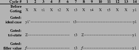
For the RTL circuit in Fig. 4(b), Fig. 9
gives the names of the variables whose values are propagated from
the multiplier to register Reg2 after gating in one iteration of
the CDFG, under four different scenarios. Z refers to tri-state
(high-impedance), X implies that the value is not yet stable or
visible at the RTL, y1' is the value of variable y1 in the
previous iteration and `-' implies that the value remains
unchanged. It is obvious that the SSA will be significantly
suppressed by gating.
Figure 9:
Cycle-by-cycle value from the gated multiplier output to
register Reg2 in Fig. 4(b).
 |
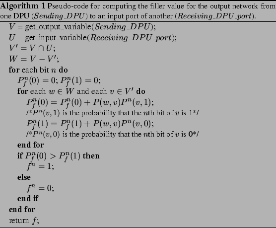
Algorithm 1 contains the pseudo-code for
computing the filler value to minimize interconnect switching
activity. Suppose the set of variables sent by DPU  (Sending_DPU) to all the DPUs in its output network is
 . Let
. Let  denote the subset of which contains all the
variables used by an input port
denote the subset of which contains all the
variables used by an input port  of another DPU
(Receiving_DPU_port). Variables in are called
desired variables for . For the RTL circuit in
Fig. 4(b), for the multiplier's output network
is {t1,t2,t3,t4,y5,y1} and its for register Reg2 is
{t3,y1}. For variables
of another DPU
(Receiving_DPU_port). Variables in are called
desired variables for . For the RTL circuit in
Fig. 4(b), for the multiplier's output network
is {t1,t2,t3,t4,y5,y1} and its for register Reg2 is
{t3,y1}. For variables  and
and  , we obtain the
probability
, we obtain the
probability  that values of
  and
and  will be output
consecutively, irrespective of their order. can be
computed by simulating the RTL circuit. Moreover, this simulation
can also yield the probability for the
will be output
consecutively, irrespective of their order. can be
computed by simulating the RTL circuit. Moreover, this simulation
can also yield the probability for the  th bit of to be 1
and 0, respectively, when is output right before or after any
variable from
th bit of to be 1
and 0, respectively, when is output right before or after any
variable from  . Let us denote these probabilities by
 and
and  , respectively. Note each value of
will have a lifetime of consecutive cycles. That is, will hold
the same value for these cycles. These consecutive cycles are
counted as one single occurrence of the corresponding value when
calculating the probabilities, because only transitions from
to will consume dynamic power. Since is not used by
and will be replaced by the filler value
, respectively. Note each value of
will have a lifetime of consecutive cycles. That is, will hold
the same value for these cycles. These consecutive cycles are
counted as one single occurrence of the corresponding value when
calculating the probabilities, because only transitions from
to will consume dynamic power. Since is not used by
and will be replaced by the filler value  , we need to decide
what should be in order to minimize the switching activity.
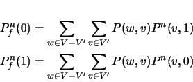
For the th bit of , say
, we need to decide
what should be in order to minimize the switching activity.
For the th bit of , say  , transitions take place when
it is different from the values of the desired variables which are
output right before or after it. The probabilities of transition
when is
, transitions take place when
it is different from the values of the desired variables which are
output right before or after it. The probabilities of transition
when is  and
and  ,
,  and
and  , are
, are
If
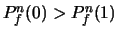 , is set to 1, othervise 0. Thus, we
can statistically minimize the bit transition activity in the
output network from DPU to port by introducing the
filler value. Since the switched capacitance is highly dependent
on switching activity in the physically neighboring wires (due to
coupling), we cannot say that the filler value thus chosen will
yield minimal spurious switched capacitance in the wires. However,
it has been found to reduce spurious switched capacitance
significantly. When the data are totally random,
, is set to 1, othervise 0. Thus, we
can statistically minimize the bit transition activity in the
output network from DPU to port by introducing the
filler value. Since the switched capacitance is highly dependent
on switching activity in the physically neighboring wires (due to
coupling), we cannot say that the filler value thus chosen will
yield minimal spurious switched capacitance in the wires. However,
it has been found to reduce spurious switched capacitance
significantly. When the data are totally random,  ,
,
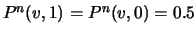 , the optimal filler value can be either 1
or 0, which reduces to the method in [61].
The overhead for setting a input to a fixed value is very low
compared to the overhead for latches. One AND gate is enough for 0
and one OR gate for 1.
, the optimal filler value can be either 1
or 0, which reduces to the method in [61].
The overhead for setting a input to a fixed value is very low
compared to the overhead for latches. One AND gate is enough for 0
and one OR gate for 1.
Next: Tri-state buffer based technique
Up: Reducing Spurious Switching Activity
Previous: Reducing Spurious Switching Activity
Lin Zhong
2003-10-11